
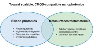
Silicon photonic platform, by leveraging the well-established CMOS fabrication, allows researchers to explore the full potential of nanophotonics while staying connected to practical applications. In our group, NYCU Silicon Nanophotonic Group (SNG), we study nanostructures, especially those compatible with mass-producible CMOS technology. This means the nanostructures we study are not only fundamentally cool and exciting to us but can make an impact on society. We like to use nanostructures to manipulate light in all aspects: guiding, bending, scattering, diffracting, enhancing, focusing, imaging and etc. We believe, in nanophotonics, “there’s plenty of room at the bottom,” as physicist Richard Feynman said about nanotechnology in 1959. In particular, we like to use the concept of metasurfaces/metamaterials. This means we design nanostructures that are small compared to the wavelength of light. So light doesn’t see the details but sees the nanostructure as a homogenized, artificial material. It is like we can create new optical materials that don’t exist in nature! The applications of our research include but are not limited to LIDAR (Light Detection and Ranging), communications, sensors, microscopy, quantum photonics, biomedical optics, imaging, and display. We summarize our research interests with the following figure:
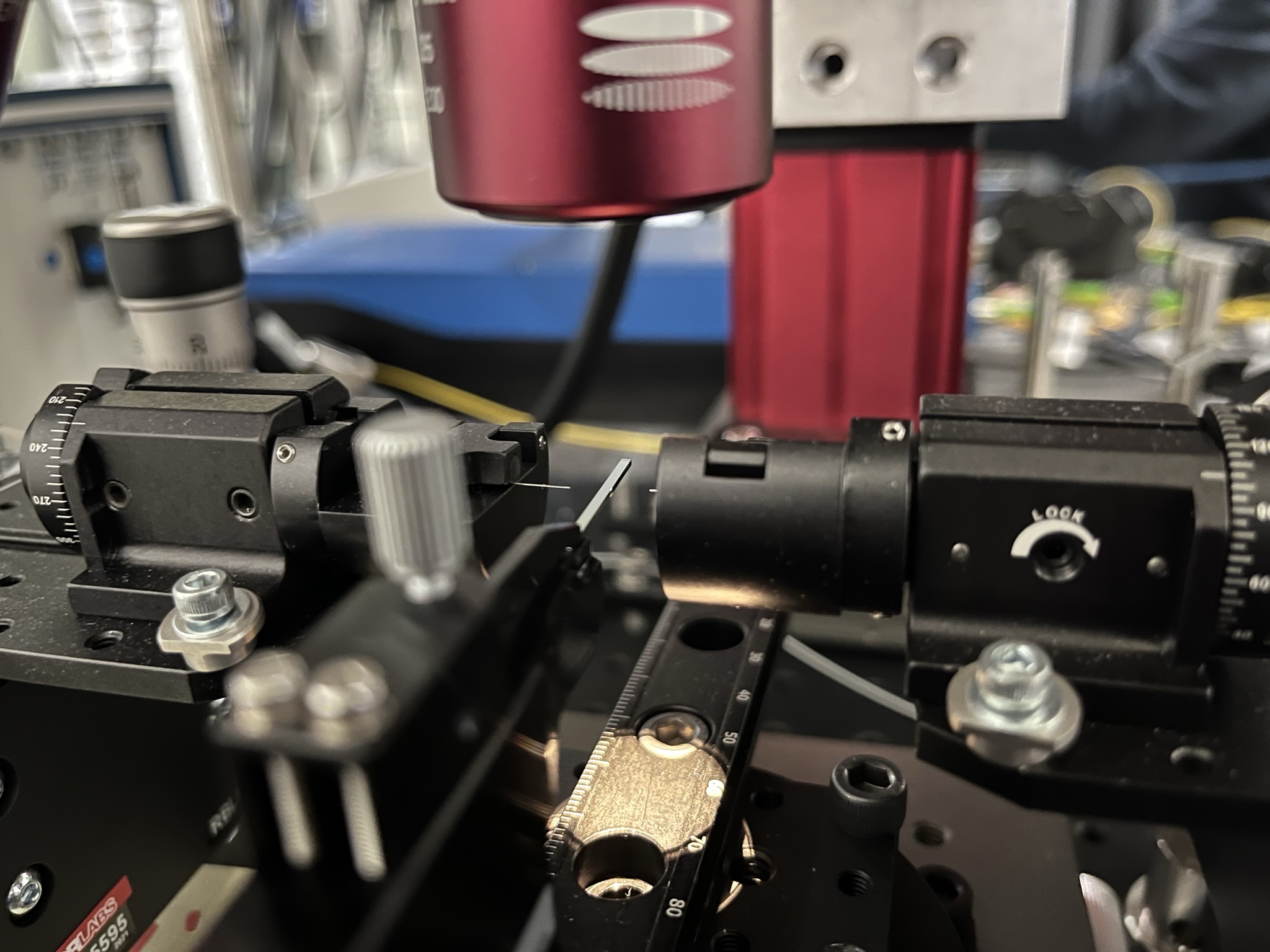
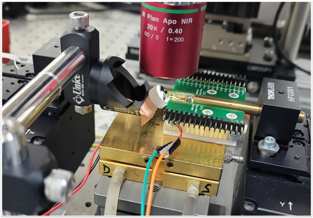
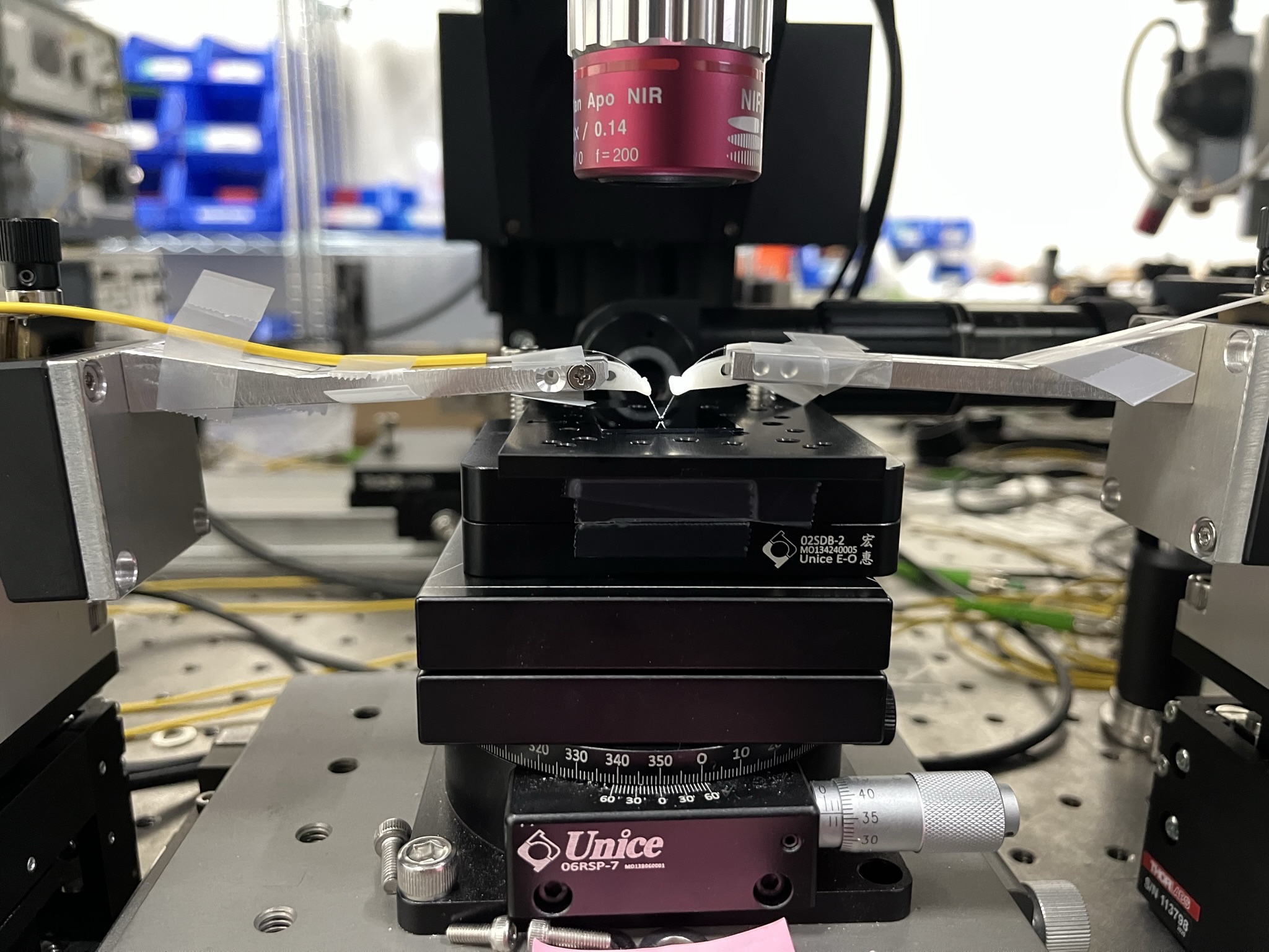
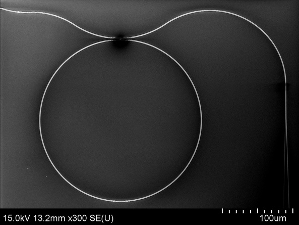
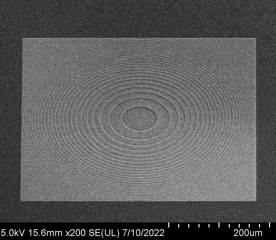
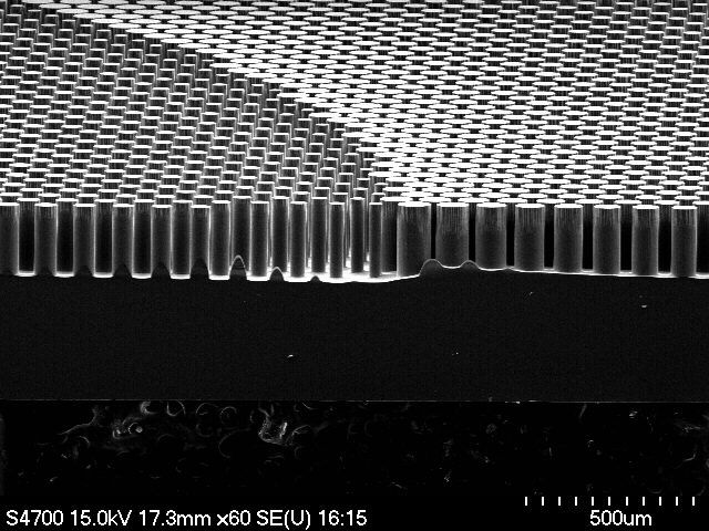
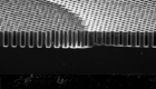
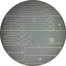
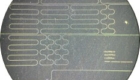
The core capabilities of our group include electromagnetic simulation, nanofabrication, and optical metrology. We use several complementary simulation methods, including finite-difference time-domain (FDTD), eigenmode expansion (EME), rigorous coupled-mode analysis (RCWA), and ray-tracing method. Our nanofabrication allows us to fabricate nanophotonic devices in-house. We have extensive experience in electron beam lithography, photolithography, plasma etching, and physical and chemical vapor deposition. In metrology, we have developed coupling techniques for silicon photonic chips, as well as microscopy, instrument control, and electronics for device testing.
在陽明交通大學矽奈米光子實驗室,我們的興趣在於理解光在奈米結構中的物理現象,並應用奈米結構去操控光的行為,如光的侷限、彎曲、散射、繞射、增強、聚焦、成像等等。我們特別著重於可相容於CMOS製程的奈米結構。這是因為在矽光子的領域中,奈米結構的使用不再只是學術上有趣的題目,更是可量產的可靠方法。我們追隨物理學家理查.費曼在1959年對奈米科技的評論:“there’s plenty of room at the bottom.” 其中我們運用超穎介面/超穎材料的概念,藉由設計小於光波波長的奈米結構,產生自然界現存材料不易達到的材料特性。本實驗室的應用方向包含包括無動件光學雷達、光通訊、微型感測器、顯微術、量子光學、生醫檢測、成像與顯示技術等。
矽奈米光子實驗室的核心能力包含奈米結構的全波電磁模擬(Full-wave electromagnetic simulation)、奈米製程、以及元件光學量測。我們使用多種模擬方法,包含有限差分時域法(Finite-difference time-domain, FDTD)、特徵模態展開(Eigenmode expansion, EME)、嚴格耦合波分析(Rigorous coupled-mode analysis, RCWA)、光線追跡法(Ray-tracing method)等。我們的奈米製程使用電子束及光學微影、電漿蝕刻、薄膜沉積等技術,具有自行製造元件的能力。在量測上,我們具有將雷射耦合至晶片的技術,並建立顯微、儀控、電子等相關設備。
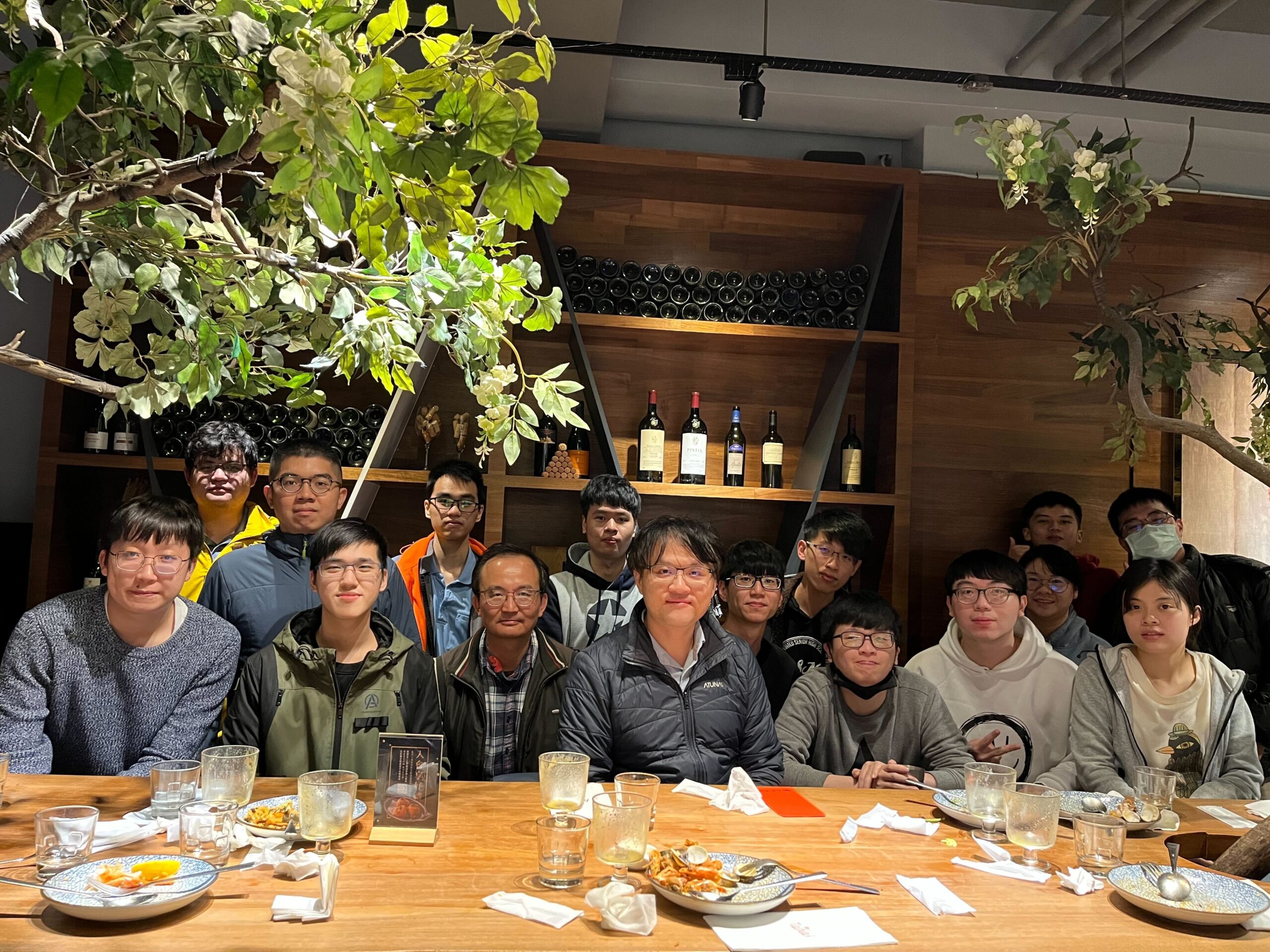
實驗室介紹影片: